|
TDA7293 Amplifier The TDA7293 is one of the two chip amps that are very popular. The other is the LM3875. What separates the TDA7293 from the LM3875 is the power stage. The LM3875 outputs are bipolars whereas the TDA7293 uses mosfets. Let’s take a closer look at what this chip amp has to offer.
At first glance, the block diagram in Fig 1 looks a bit confusing. It took me a while to figure out what it’s all about. Having studied it closer, there are some very interesting features. BootstrapFirst and foremost is the “bootstrap” at pin 6. The TDA7293 uses this method instead of a current source. The capacitor that is used for bootstrapping can be wired to the output of the amp (pin 14) or to a special bootstrap loader at pin 12. For normal use, bootstrapping from the output (pin 14) is perfectly fine. Mute & StandbyThe next feature that got me puzzled is the MUTE and STANDBY pins at 10 and 9. They appear to be redundant but they are there. I would use the TDA7293 in Play mode all the time but should one decide to have the amp in Standby, it can be done. What this means is that the voltage and power mosfets are probably “OFF”. I will need to design a sub-circuit to sense the presence of an input signal so that the amp “comes alive” automatically. The MUTE switch basically disconnects the source from the input. I can design it such that the TDA7293 has no sound when over driven. To accomplish this, I use a detector that activates the Mute switch when the amp is driven to clipping. This will prevent the TDA7293 from blowing up. These two features are nice to have but a bit too complicated for DIY. They are more helpful in a commercial product. High EfficiencyA unique feature of the TDA7293 regards the power rails. There are actually four pins supplying power to the TDA7293. Two go straight to the power mosfets (pins 13,15) while the other two (pins 7,8) are for the voltage amp. They are not linked internally. The purpose of this separation is when the TDA 7293 is wired for “high efficiency”.
Fig 2 shows the TDA7293 with split power rails. Notice pins 13 and 15 operate on two rail voltages. For lower power output, it’s from the +-25V rails. When it exceeds a certain output, it switches to +-50V. This is similar to Class H. The voltage amp, however, is always at +-50V. (pins 7,8). Personally, I’m not keen on using the TDA7293 this way. That’s because I can easily design a discrete Class AB power amp working at +-50V rails. In doing so, I avoid the complexity and switching artifacts associated with Class H. Modular
I saved the best for last. What they call Modular is really using two TDA7293, one as Master while the other as Slave. In this arrangement, only the power mosfets in the Slave are used. We can think of this as extending the number of power mosfets in the output stage. This is done via pin 11, the Buffer Driver. With this arrangement, I can run the TDA7293 at +-40V without clipping the amp when it sees 4 ohms. If I were to design a single TDA7293 to cater to 4 ohm load, I will have to use +-28V.. This concludes my review of the TDA7293. I have tested this amp a few years ago and I can’t find anything objectionable. It is an outstanding performer. I will be designing a pcb for this chip amp soon. TDA7293 Power OutputThe TDA7293 is touted as a 100-Watt amplifier which I find questionable. Please note that this power is at 10% THD into 8 ohms. People who are serious with audio do not listen at 10% THD because that’s into heavy clipping territory. In fact, most would avoid clipping entirely. What I’m interested in is the power output just before clip. When I test out my new TDA7293 pcb, I will know exactly what the maximum clean power is |

February 2, 2022Amplifiers, Projects
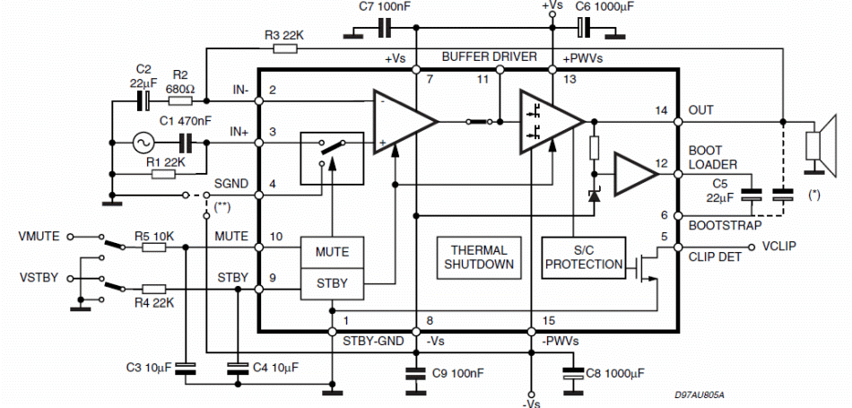
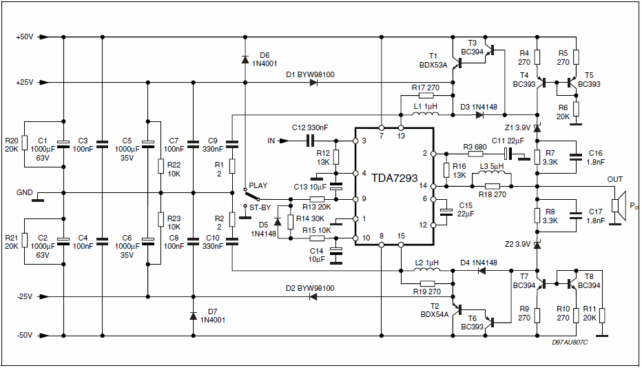 Fig 2 – TDA7293 High Efficiency Circuit
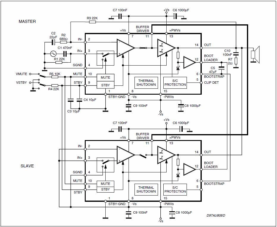 Fig 3 – TDA7293 with Slave