|
LM3886TF – Bench Testing
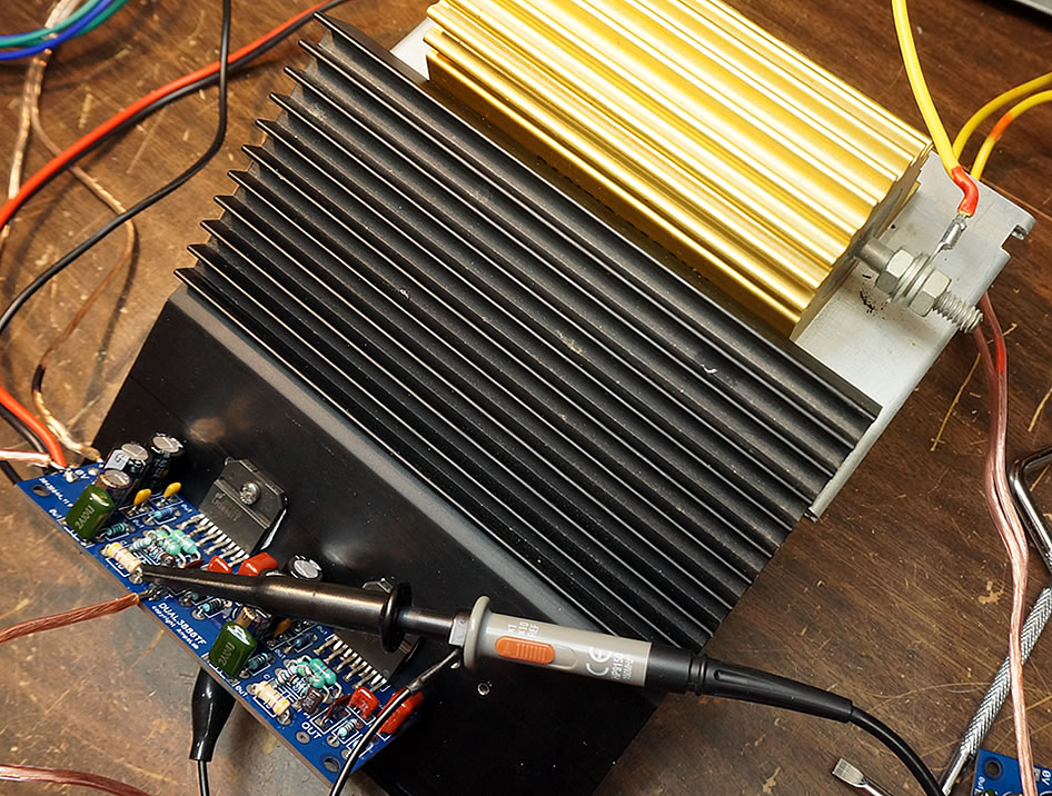
The Dual LM3886TF is finally ready for testing. I was looking around for a heatsink and found one from a Crown DC150 which has a nice flat surface. Drilled two holes, tapped M3 threads, applied thermal compound and bolted the LM3886TF onto it. Soldered in my bench power supply, signal generator and a high powered dummy load. The supply rails were adjusted for +/- 28Vdc. This is the recommended voltage for 4Ω. I do not recommend +/- 35V which is for 8Ω because speakers with nominal impedance of 8Ω sometimes drop to 4Ω. When that happens, the “SPIKE” circuitry in the LM3886TF will activate, resulting in very unpleasant music.
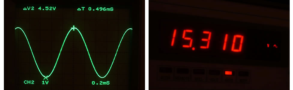
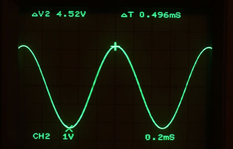
The plot on the left is the LM3886TF at Full Power into 8Ω. The output voltage is 15Vrms. That converts to 28Watts, very close to the 30W in their datasheet. Input from signal generator is 0.7Vrms. This is almost 0dBu (0.775V). It will work well with mixers referenced to dBu. The plot on the right is what the LM3886TF looks like when over-driven. It won’t get any louder, just distortion. Avoid this at all cost. If the LM38876TF is not loud enough, use a more powerful amplifier.
Next is the Square Wave test. This is a very important test as it will flag any issues with the amplifier. Again, the load is 8Ω. The display on the left is a 10kHz Square. The trace is beautiful. Clean. No breakups on the leading and trailing edges. No oscillations at the top and bottom. Rise time is at 2.4us, measured at 10% to 90% of full scale (10V peak to peak). With the 10kHz Sq concluded, I proceeded with the 20kHz. This is the icing on the cake. The display on the right shows a 20kHz Sq wave at 10V peak to peak. Rise time is 2.0us. No overshoot is observed at the leading and trailing edges. There’s a gentle knee at the top followed by a very slight downward tilt. This is my preferred target response of a 20K Square wave.
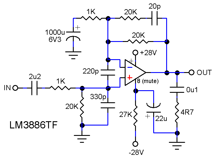
The LM3886TF circuit is simplicity in itself. It looks like your typical op amp. The values above are what I used for my LM3886TF. Follow this and you’ll get the performance shown in the plots above. Here are the specs of the LM3886TF. Power Output = 28W into 8Ω | 60W into 4Ω Power Supply Specs In the schematic above, astute readers will notice the muting resistor is 27K. This will draw 1mA out of pin 8, double the minimum of 0.5mA recommended. With 27K, it did not trigger any false muting when I drove it to full power. Thinking aloud, this muting feature can be used to shut off the LM3886TF when it is subjected to clipping or to prevent damage from overheating. I will need to design additional circuits for these but it’s feasible. It’s not as convenient as my hybrid IA502 kit though. That amplifier is built around the TDA7250 which has those features built-in. Drive the amp to clip and it shuts off. Bullet proof. The Dual LM3886TF pcb will be available for purchase soon. I made slight changes to the pcb, hence the reason for another lot from my pcb maker. The pcb will likely be sold with 2 pcs of genuine LM3886TF. This will avoid complaints about the pcb which in fact, the cause is the user installed fake LM3886TF. |
March 13, 2022Electronics, Projects
 Full Power into 8Ω = 28Watts @ 1kHz Sine
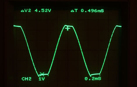 Clipped Waveform into 8Ω
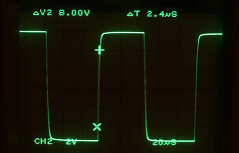 10kHz Square Wave into 8Ω
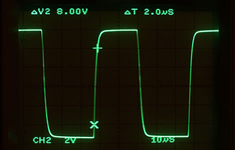 20kHz Square Wave into 8Ω