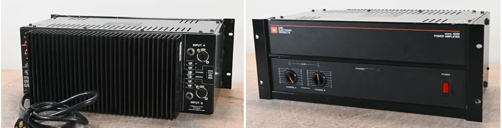
JBL 6260
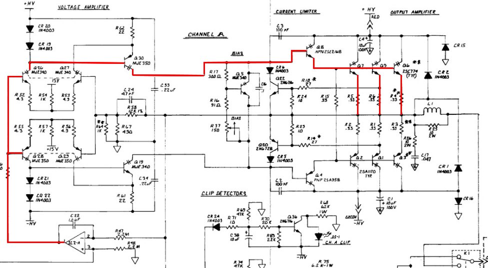
Apart from being solidly build, what can we glean from her schematic. JBL 6260 Power Amplifier The JBL 6260 has a mirror image typology, that is the top and bottom halves are similar (Fig 1). An op-amp drives the positive and negative input differentials and at the same time, it serves as a DC Offset Servo. The VAS is driven by the positive side of the differential (Red line). No darlingtons are used. After the VAS, a driver drives 3 power output transistors (2SC2774/2SA1170). These are the Sankens in MT-200 packing. Summary While the basic circuit is proven, I question the use of MJE340/350 for the input differentials. I feel small signal transistors are more suitable here. Also, the same transistors are used in the VAS. While there’s nothing wrong with that, the MJE340/350 are not highly regarded for sound quality. The only redeeming feature is their high Vceo of 300V. However, they are popular in PA amps but some HiFi owners find them a bit bright or rough. This is of course a personal opinion but transistors do affect the sound quality in audio. When I have the time to work on these amplifiers, I will likely upgrade some transistors. After that, I will “voice” the amplifier for my signature sound. Like all things in audio, there’s the technical aspect after which comes the art. That’s what separates the great ones from the ordinary. |
August 4, 2025Amplifiers, Electronics